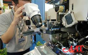
Taiwan Semiconductor Manufacturing Company showcased its latest semiconductor and packaging technologies at the 2026 Taiwan Technology Symposium in Hsinchu, highlighting progress in next-generation chip production and AI-driven computing.
The company introduced its A13, A12, and N2U process technologies while announcing mass production this year of what it described as the world’s largest chip-on-wafer-on-substrate (CoWoS) packaging solution. TSMC said its 5.5-reticle-size CoWoS technology has achieved yields exceeding 98%.
To support growing demand for AI and advanced chips, TSMC plans to launch five new fabs in 2026 and expects its 2nm production capacity to grow at a compound annual rate of 70% between 2026 and 2028. Capacity for CoWoS and SoIC advanced packaging is also projected to expand by more than 80% annually through 2027.
TSMC added that its A16 process remains on track for production in the second half of 2026, while approximately 25 customer 2nm chip designs have already been finalized with more than 70 additional projects in development.